Printed Circuit Board Designers deal with an array of challenges, from electrical, functional, mechanical,
production, quality and price. To avoid some common problems, Design for Manufacturability
(DFM) considerations should also be factored into the design process. Some of the
most common DFM problems are discussed below, along with some alternative considerations.
Footprint Geometry
Try to refer to standard IPC-based footprint designs, or manufacturer recommended
footprints, to ensure components can be placed and soldered without errors.
Component Selection and Placement Location
As designers try to minimize through hole (THT) components on new designs. It’s
a good suggestion to try and locate them all on one side of your circuit board.
This allows for wave-soldering and avoids more expensive selective soldering processes.
Connection Direction for SMD Components
If possible, avoid connecting 2 SMD pads in, near, or under, a SMD component as
this may cause problems during testing or inspection. During Automated Optical Inspection
(AOI), the camera may not be able to detect a short because an intended connection
may interfere.
Balanced or Even Connection of Component Pads
Uniform connections for SMD components, especially small components like 0402, 0201,
etc., are critical to avoid “tombstoning.” This refers to components partially,
or completely, lifting off the surface of a PCB board during reflow. Uniform connections
to BGA pads is also critical to assure reliable solder results, otherwise the cost
of test, inspection and repair may increase.

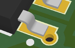
Vias / SMD Pads
Avoid the common mistake of adding vias within pads which can lead to a weak solder
joint and circuit damage during soldering.
Copper Distribution
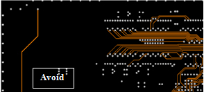
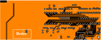
Stranding or isolating a single, thin trace from higher density copper areas creates
more difficulty in the copper etching process so as much as possible, keep copper
distribution even across each layer to improve processing and yields.
Via or Layer Offset
PCB fabrication, as all manufacturing processes, has inherent tolerances in each
process. Typically Printed Circuit Board manufacturers drill PCBs in stacks or multiple groups rather
than sequencing individually. To improve process yield, and reduce cost, consider
your minimum annular ring size, or pad geometry (teardrop vs round) to make your
product more robust and improve yields by compensating for process tolerances.


Solder Mask
To avoid mask skips between pads, maintain a minimum distance of 75 µm (3 mils)
between features to ensure complete mask fill.

Unconnected Via Pads
PCB fabricators are able to preserve drill tool life by removing unconnected or
unused inner layer via pads. From an electrical standpoint, this may have no effect
on the final product, but if the designer doesn’t want them removed, it’s best to
note in your design or fabrication drawings/specifications.
Hole Size Tolerances
Specify the tolerance of hole dimensions to ensure proper fit of plated-through-hole
(PTH) components and specify clearly for fabrication. Component datasheets list
plus/minus tolerances to accommodate variations in aging, wear, temperature, plating
material, machining, etc. When holes are drilled, bits wear, or may vibrate slightly
in a hole causing a slightly larger hole. Then holes are plated and may have thickness
variations from batch to batch, or location on the board. A good rule of thumb to
accommodate for all of these factors is to make your drill hole 0.007 inches larger
than the part lead diameter to accommodate all tolerances, drill wear / wobble,
and plating variations.
DFM issues present another set of challenges and opportunities for successful product
design. Following the above hints will improve placement, stack-up, and mask to
help achieve your desired goals. Let our experienced team of engineers, and designers
help you with these or other questions to help you realize your product objectives.