It’s easy to leave the PCB design guidelines as an afterthought, spending most of your time focusing on circuit design, functionality, and component selection. However, not providing attention to PCB layout basics can lead to a design that translates poorly from the digital domain to physical reality. Thereby making it more difficult to fabricate.
The top 5 PCB design guidelines we can suggest to improve manufacturability, functionality, and reliability are discussed below.
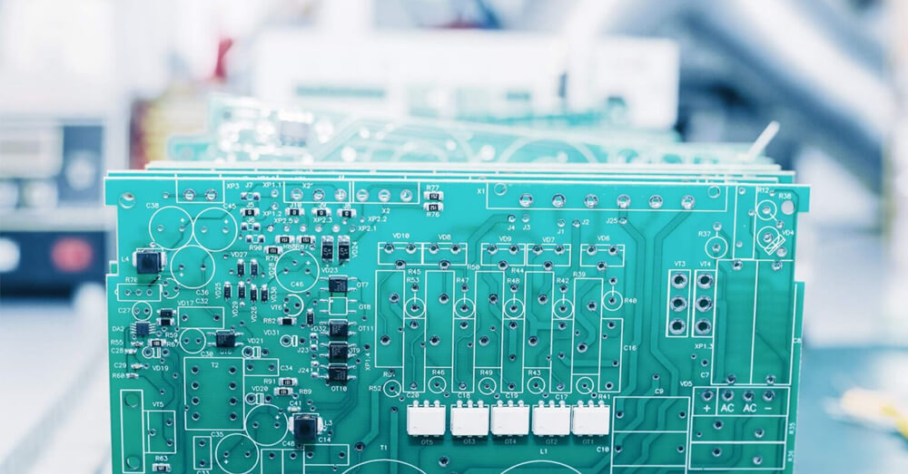
1. Fine-Tune Component Placement
The component placement requires strategic consideration of the available PCB real estate available on your board. This process can be challenging. However, placement of electronic components will determine how easy the board is to manufacture, as well as how well it meets your design requirements.
There are many PCB layout rules to consider during component placement. While general board layout guidelines tell you to place components in order of connectors, power circuits, precision circuits, critical circuits, etc, there are also several specific board layout guidelines to consider.
Orientation: Be sure to orient similar components in the same direction as this will help with effective routing in PCB design. It also helps ensure an efficient and error-free soldering process during assembly.
Placement: Avoid placing components on the solder side of a board that would rest behind plated through-hole components.
Organization: It’s recommended to place all your surface mount devices (SMD) components on the same side of your board according to SMD PCB design rules. All through-hole (TH) components should be placed on the top side of your board to minimize the number of assembly steps.
When using mixed-technology components (through-hole and surface mount components), manufacturers might require an extra process to assemble your board, which will add to your overall printed circuit board costs.
2. Power, Ground & Signal Traces
After component placement, route your power, ground, and signal traces to ensure your signals have a clean and trouble-free path of travel. Here are some guidelines to keep in mind for this stage of your layout process:
Place your power and ground planes internal to your printed circuit board keeping them symmetrical and centered. This will help to prevent your board from bending, which will also affect whether your components are properly positioned. Note that this is not possible on a two-layer board as you will not have any room for components. To power your ICs, it’s recommended to use common rails for each supply, ensure you have solid and wide traces, and also avoid daisy-chaining power lines from part to part.
Next connect the signal traces to match your schematic guidelines. PCB layout best practices recommend that you always keep traces as shortand directas possible between components. If your component placement forces horizontal trace routing on one side of the board, then always route traces vertically on the opposite side.
Printed circuit board design rules and PCB layout guidelines become more complex as the number of layers in your stack-up increases. Your routing strategy will require alternating horizontal and vertical traces in alternating layers unless you separate each signal layer with a reference plane.
Your printed circuit board design will likely require different nets that will carry a wide range of currents, which will dictate the required net width. It’s recommended to provide a 0.010” width for low current analog and digital signals. Printed circuit board traces that carry more than 0.3 A should be wider.
3. Keep Things Separate
Large voltage in power circuits and current spikes can interfere with low voltage and current control circuits. To minimize this interference issue, it’s recommended to:
Separate power ground and control ground for each power supply stage. If you do have to tie them together in your PCBs, make sure it’s toward the end of your supply path.
If you have placed your ground plane in the middle layer be sure to place a small impedance path to reduce the risk of any power circuit interference and to help protect your control signals. The same guideline can be followed to keep your digital and analog ground separate.
To reduce capacitive coupling due to the placement of a large ground plane and the lines routed above and under it, try to have your analog ground crossed only by analog lines.
4. Minimize Heating Issues
Heat dissipation can degrade performance. Some guidelines to minimize include:
Identify Problem Parts -considerwhich components will dissipate the most heat on your board. This can be accomplished by first finding the “Thermal Resistance” ratings in the component’s datasheet, and then following the recommended guidelines to divert the heat being produced. Of course, heatsinks and cooling fans can be added to keep component temperatures down. Keep critical components away from any high heat sources.
If you have more than one component that generates a large amount of heat, it may be best to distribute these components throughout the board, rather than clustering them in one location. This prevents hot spots from forming in the board. You may have to carefully balance the placement of these components against keeping trace lengths short as you devise a routing strategy, which can be challenging.
Thermal reliefs can be useful to produce a manufacturable board and they are critical for wave soldering application on assemblies and multilayer boards with high copper content. Because it can be difficult to maintain process temperatures, it’s always recommended to utilize thermal reliefs on through-hole components to make the soldering process as easy as possible by slowing the rate of heat sinking through the component plates.
Some designers advise using a thermal relief pattern for any via or hole that is connected to a ground or power plane. This is not always the best advice. Note that a power/ground via can appear near an IC with a fast switching speed, which generates a lot of heat. Moving heat away from the IC helps regulate the temperature of the IC.
The ground plane can act as a large heat sink that then transports heat evenly throughout the board. Therefore, if a particular via is connected to a ground plane, omitting the thermal relief pads on that via will allow heat to conduct to the ground plane. This is preferable to keeping heat trapped near the surface. However, this can create a problem if your board is assembled using wave soldering, as you need to keep heat trapped near the surface.
In addition to thermal reliefs, you can also add teardrops where traces join pads to provide additional copper foil /metal support. This will help to reduce mechanical stress and thermal stress.
5. Verify Your Layout Against Your PCB Design Rules
It’s easy to get overwhelmed as you scramble to fit your remaining pieces together for manufacturing. Double and triple-checking your work for any errors at this stage can mean the difference between a manufacturing success or failure.
To help with this quality control process, it’s always recommended to start with your Electrical Rules Check (ERC) and Design Rules Check (DRC) to verify you’ve met all of your established constraints. With these two systems, you can easily define gap widths, trace widths, common manufacturing requirements, high-speed electrical requirements, and other physical requirements for your particular application. This automates PCB layout review guidelines for validating your layout.
Note that many design processes state that you should run design rule checks at the end of the design phase while preparing for manufacturing. If you use the right design software, you can run checks throughout the design process, which allows you to identify design potential problems early and correct them quickly.
When your final ERC and DRC have produced error-free results, it’s then recommended to check the routing of every signal and confirm that you haven’t missed anything by running through your schematic one wire at a time. And of course, ensure that your PCB layout matches your schematic with the use of your design tool’s probing and masking feature.
Optima Technology is a global provider of PCBs, PCB Assemblies, Cables and System Assemblies located in Lewisberry, PA and New Delhi, India. Since 1995, Optima has specialized in providing local support coupled with cost-effective pricing via offshore manufacturing through our ISO approved facilities. Please reach out to optima@optimatech.net if you’d like to discuss further your PCB or Electronic Assembly needs.