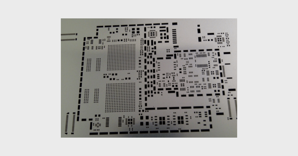
A critical aspect of any PCBA surface mount assembly process is the proper application of solder paste to the printed circuit board (PCB) in order to make sure component terminals are applied correctly to the PCB pad to ensure proper and well-maintained electrical connections. Generally this process is achieved through the use of a solder stencil which is usually made out of stainless steel and has openings (apertures) through which solder paste can be deposited precisely where needed and in the exact quantities for your unique PCB design.
Some of the key design features of an effective solder paste stencil are:
- Thickness
- Size of the apertures
- Material of the stencil
- Alignment
- PCB Design
Stencil Thickness
This ensures the proper volume of solder paste is released. Stencils are typically .004-.008 inches. If the stencil is too thick relative to the size of the holes then the paste may be get held in the inner walls of the apertures
Aperture size
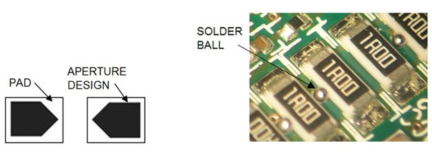
To provide a good seal between the stencil and PCB, apertures are typically .002 inches smaller on all sides than the PCB component pads. If the size is not correct, solder defects can occur such as bridging and solder beads. Some apertures need a special design to deposit less paste on the inner edge of the part to reduce the possibility of ‘mid-chip’ solder balls forming. Below is an example of a possible solution known as ‘home-plate’ apertures and a photo of ‘mid-chip’ solder balls.
Material of the Stencil
Different materials impact the stencils ability to release solder paste from the apertures. While stainless steel is most commonly used, nickel can be used as an alternative for PCB designs that have fine pitch devices (although at a higher cost). You can also apply a coating to the metal like NanoProTek to improve the release of paste from the apertures.
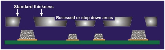
When PCB designs contain a large variety of parts, including fine pitch devices that require a thin stencil and larger parts which require a thicker stencil, a multilevel or ‘stepped’ stencil can be employed.
Step-up areas are used to increase the volume and height of the solder paste in selected areas by adding material to the stencil. Step-down areas are created by removing material from the stencil and are used to reduce the volume and height of the solder paste deposit in selected areas. To print successfully, apertures must be designed to be a minimum distance from the step edge. The distance is dependent on the step dimensions and is known as the ‘keep out area’.
Alignment
In order to accurately print solder paste to the PCB pads, registration marks or ‘fiducials’ should be added to the PCB and the stencil.
PCB Design
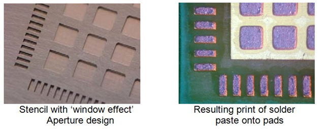
If the PCB design has large copper pads underneath a component (typically to provide secure electrical connection and heat dissipation) this can cause issues if the entire pad has solder paste applied to it, resulting in the device being lifted and the outer leads not connecting well. This can be overcome by creating a ‘window effect’ in the stencil aperture design to reduce the solder volume (shown below).
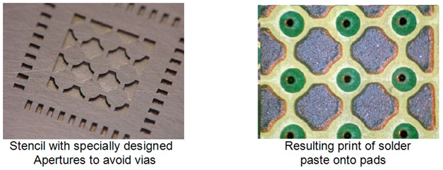
Another PCB design feature on the same type of device that can cause undesirable solder results is when there are vias within the large copper pad for heat dissipation. In this case the stencil apertures should be specially designed to avoid the solder paste from being deposited onto the vias.
It is critical to use a stencil that is designed with every possible point considered in order to achieve proper, repeatable printing results.
Optima Technology is a global provider of PCBs, PCB Assemblies, Cables and System Assemblies located in Lewisberry, PA and New Delhi, India. Since 1995, Optima has specialized in providing local support coupled with cost-effective pricing via offshore manufacturing through our ISO approved facilities. Please reach out to optima@optimatech.net if you’re interested in learning more.