PCBs, which are used in virtually all electronic devices, essentially routes electrical signals to satisfy the product’s electrical and mechanical circuit requirements. This is accomplished through a network of copper paths. To help prevent product designers from making unnecessary errors at least an awareness of the manufacturing complexities for PCBs is warranted.
Step 1:
PCB design software (such as Altium Designer, OrCAD, Pads, KiCad, Eagle, etc.) are used for design of PCBs to ensure they are compatible with manufacturing capabilities.
Upon design completion and approval, the design information can be exported into files to be used for manufacturing in formats supported by the PCB Manufacturer. These are generically called “gerber files.”
Gerber files encode comprehensive details defining copper traces, drill hole definition, copper feature apertures, component designators, and other information. The software performs oversight algorithms to ensure there are no errors created by the designer. After a comprehensive review and approval, the files are sent to the PCB Manufacturer for production. To ensure the design, fits with the manufacturer’s minimum tolerance capability, the printed circuit board supplier a Design for Manufacturability (DFM) review before starting fabrication. Any concerns or issues will be communicated back to the designer for resolution. Only after a successful DFM review is complete, will the production operations commence.
Step 2:
After completion of the design output, and manufacturers conduct a DFM check, PCB printing can begin next. Manufacturers use a plotter (i.e. printer), to make photo films of the PCBs, for printing and fabrication of circuit boards. The photo films image the individual layers of the PCBs. Although it’s a laser printer, it isn’t a standard laser jet printer. Plotters use incredibly precise printing technology to provide highly detailed films.
The final product results in a plastic sheet with a photo negative of the PCB in black which represents the conductive copper parts of the PCB for the inner layers. The remaining clear portion of the image denotes the areas of non-conductive material.For the outer layers the opposite pattern is followed: clear for copper, black the areas to etch away.
Each layer of PCB and solder mask receives its own clear and black film. For example, a two-layer PCB needs four films (two for the layers and two for the solder mask). All the films have to correspond perfectly to each other to maintain correct alignment.
Further, registration holes are punched through all films to maintain correct alignment of all films. An alignment table is used to perform small calibrations to generate the optimal match of the layers before punching is performed. These punched holes are used for alignment/registration pins in the imaging process.
Step 3:
Inner layer printing.
The photo films prepared in the previous step, create a figure of all copper paths, which now need to be printed onto the copper foil of the PCB laminate layers.
Each PCB is comprised of a laminate board consisting of an epoxy resin core/glass fiber substrate. This substrate provides a sturdy and dust-resistant starting point for the PCB. Copper is pre-bonded on both sides of the substrate. So photo lithography techniques are used to remove the excess copper (i.e. a subtractive process) to leave the desired design or copper paths from the films.
The copper-sided laminate is well-cleaned and passed into a decontaminated environment. During this stage, it’s vital that no dust particles settle on the laminate. An errant speck of dirt might otherwise cause a circuit to be defective creating either an electrical short or open connection.
Next, the panel receives a layer of photo-sensitive film called photo resist. The photo resist comprises a layer of photo reactive chemicals that harden after exposure to ultra violet light. This ensures an exact match from the photo films to the photo resist.
After, the film and board line up and are exposed to UV light. The light passes through the clear parts of the film, hardening the photo resist on the copper underneath. The black ink from the plotter prevents the light from reaching the areas not meant to harden so they can be chemically removed or etched away.
After UV exposure, the board is washed with an alkaline solution to remove any photo resist left unhardened. A pressure wash removes anything else left on the surface. The board is then dried.
The product emerges with resist properly covering the copper areas meant to remain in the final form. A technician examines the boards to ensure that no errors occur during this stage. All the resist present at this point denotes the copper that will emerge in the finished PCB.
This step only applies to boards with more than two layers. Simple two-layer boards skip ahead to drilling. Multiple-layer boards require further processing steps.
Step 4:
After photo resist removal, the hardened resist covering the copper to keep, a chemical process is used to etch away excess copper. The copper solvent solution bath removes all of the exposed copper. The desired copper remains fully protected beneath the hardened layer of photo resist.
Once the solvent removes the unwanted copper, the hardened resist protecting the preferred copper is removed using another solvent. The result is a board with only the copper substrate necessary for the particular PCB design.
Step 5:
When all the individual layers are clean and ready, alignment/registration punches are needed to ensure they line up properly. The registration holes align the inner layers to the outer ones. An optical punch machine is used to hold the alignment and punch the holes.
Once the layers are placed together, it’s impossible to correct any errors occurring on the inner layers. Another machine performs an automatic optical inspection of the panels to confirm a total absence of defects. The original design from Gerber, which the manufacturer received, serves as the model. The machine scans the layers using a laser sensors and electronically compares the digital image with the original Gerber files.If the machine finds inconsistency, the comparison is displayed on a monitor for the technician to review and approve/reject.Once the layer passed inspection, it moves to the final stages of PCB production.
Step 6:
Here the final PCB will start to take shape as all the separate layers are joined together. This is a two-step process, layer stack and bonding.
The outer layer material consists of sheets of fiber glass, pre-impregnated with epoxy resin, called prepreg. A thin copper foil covers the top and bottom of the substrate, which contains the etched copper traces.
To sandwich them together a heavy metal table with metal clamps is employed. The layers securely fit into registration pins in the table. Everything must fit snugly to prevent shifting during alignment.A prepreg layer is placed over the alignment basin. The substrate layer fits over the prepreg before the copper sheet is placed. Further sheets of prepreg sit on top of the copper layer. Finally, an aluminum foil and copper press plate is added to complete the stack.
An automatic routine run by the bonding press computer performs the process of heating the stack, applying pressure, and controlling the cool down cycles.
Step 7:
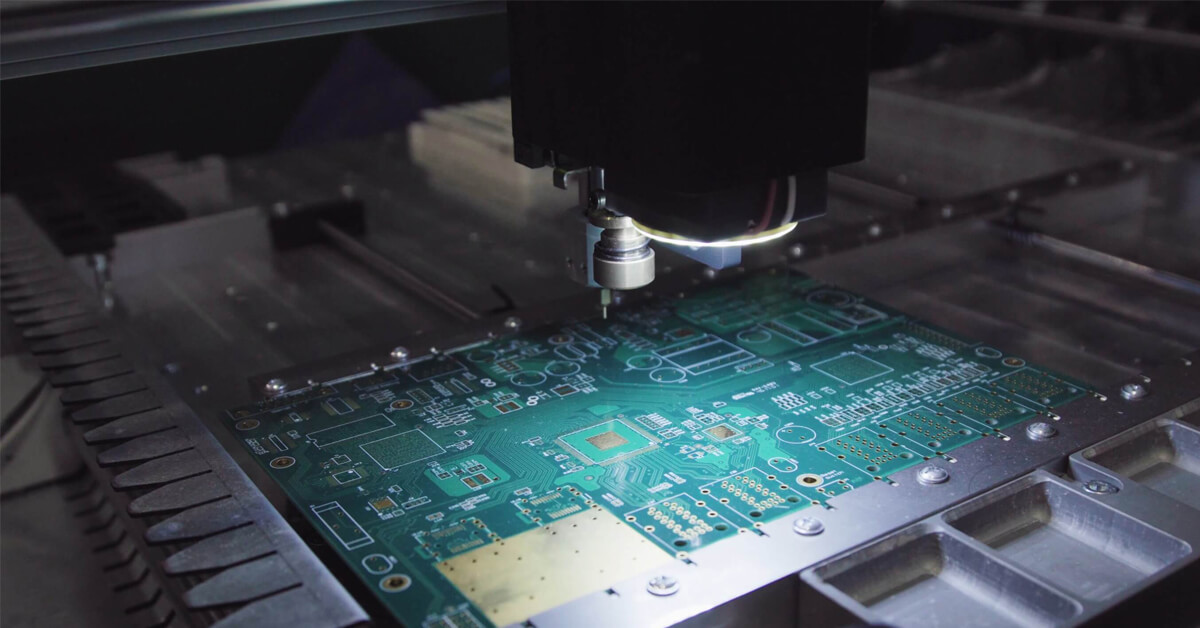
Drilling-holes are machined (drilled) into the stacked bonded boards. The precision of vias, component placement of leaded devices, etc. all depend on this operation. Location of drill targets are found using an x-ray locator. Then, proper registration holes are bored to secure the stack for the series of drilling.
Next a buffer material is placed beneath the drill target to ensure a clean bore is produced. This exit-material prevents any unnecessary tearing upon the drill’s exit. A computer controlled drill operation is used to manage every movement of the drill. The computer-driven machine operation uses the drill file output from the original design software package to identify the proper spots to bore.
The drills use air-driven spindles that turn at 150,000 rpm. An average PCB often contains well over one hundred drill hits. During drilling, each needs its own special moment.
Step 8:
After drilling, the panel goes into plating. After a thorough cleaning, the panel undergoes a series of chemical bath where chemical deposition processes deposit thin layers of copper over the surface of the panel and into the drilled holes.
The copper baths completely cover, or plate, the walls of the holes while the entire panel receives a new layer of copper. The entire process (time, temperature, bath chemistry, etc.) are all computer controlled.
Step 9:
Like in the previous Step 3, a photo etch was applied to the panel, in this step it’s repeated. This time, the outer layers of the PCB are imaged with their design. In a sterile room to prevent any contaminants from sticking to the layer surface, a layer of photo resist is applied to the panel. The prepped panel is exposed to cure the photo resist taking care to not affect the photo resist.
Black ink transparencies are secured by pins to prevent misalignment with the panel. The panel and stencil is then exposed to UV light to harden the photo resist. The panel then passes into a machine that removes the unhardened resist. This is the reverse process used for the inner layers.
Step 10:
Next, returning to the plating operations. The panel is electroplated with a thin layer of copper. The exposed sections of the panel from the outer layer photo resist stage receive the copper electro-plating. Following the initial copper plating baths, the panel usually receives tin plating, which permits the removal of all the copper left on the board slated for removal. The tin guards the section of the panel meant to remain covered with copper during the next etching stage. Etching removes the unwanted copper foil from the panel.
Step 11:
Final Etching-The tin deposited in the previous step protects the desired copper during this stage. The unwanted exposed copper and copper beneath the remaining resist layer undergo removal. Again, chemical solutions are applied to remove the excess copper. The conducting areas and connections are now in tact.
Step 12:
Before the solder mask is applied to both sides of the board, the panels are cleaned and covered with an epoxy solder mask ink. Again, UV light is employed, and it passes through a solder mask photo film. The covered portions remain unhardened, to be removed. Then the board is passed into an oven to cure the mask.
Step 13:
Chemical plating is used to add gold or other solderable finishes at this step.
Step 14:
Ink jet printing is used to deposit silk screen onto the surfaces of the board. This is used to indicate important information related to the PCB, such as manufacturing information, location designators to aid further assembly, etc.
Step 15:
Electrical tests are performed on the PCB to confirms functionality and conformity to design requirements.
Step 16:
The last steps involve machining operations to profile and or V-Score PCBS.Individual circuit boards are cut from the panel, or partially removed to simplify separation following subsequent assembly operations. Methods involve computer controlled routers or v-groove cutters. A router leaves small tabalong the board edges while the v-groove cuts diagonal channels along both sides of the board. Both ways permit the boards to easily pop out from the panel.
Summary
A lot of work goes into manufacture or fabrication of a printed circuit board.To ensure your boards are produced with your required quality, select a manufacturer capable of meeting your requirements.
Optima Technology is a global provider of PCBs, PCB Assemblies, Cables and System Assemblies located in Lewisberry, PA and New Delhi, India. Since 1995, Optima has specialized in cost-effective products and services. Please reach out to optima@optimatech.net if you’d like to discuss further your PCB, Electronic Assembly needs, or request a quote!