With the increasing complexity of Printed Circuit Board (PCB) assemblies, it has become more common for surface mount components to be designed on both sides of the PCB. This provides challenges when automating the soldering of the through-hole components.
Typically components that need to be soldered are done so using ‘Wave Soldering’ (the preferred method), however this process is not always possible due to complexities in the assembly design.
In these cases the components are usually hand soldered but this can causes inconsistent results leading to quality problems. These can be time consuming to solve and increase manufacturing costs and lead times.
As a result, many companies have turned to Selective Soldering as an alternative method because it is faster (reducing manufacturing costs and lead times) and there are less quality concerns than traditional hand soldering.
Selective Soldering
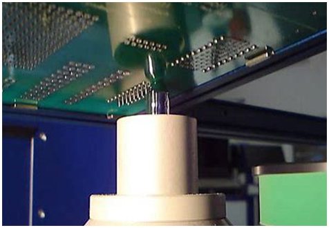
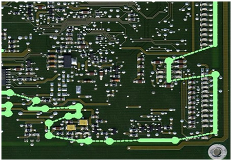
Selective soldering is a process of soldering selected electronic components to a PCB. The components are selected by way of a program that is created using an image of the PCB specifying where flux and solder are to be applied.

Similar to wave soldering, selective soldering is done by preheating, applying flux, and soldering. In both processes, the temperature of the assembly is raised before soldering (preheating). While in wave soldering the entire PCB is coated, in selective soldering the application of flux is only to the components that are to be soldered. In both processes the PCB is exposed to a molten wave of solder. In wave soldering the entire board is passed over the wave, while in selective soldering, only individual connections see the wave (one after the other). Selective soldering is a slower process than wave soldering but it is much more precise and it allows independent configuration of the soldering of each position.
Optima Technology is a global provider of PCBs, PCB Assemblies, Cables and System Assemblies located in Lewisberry, PA and New Delhi, India. Since 1995, Optima has specialized in providing local support coupled with cost-effective pricing via offshore manufacturing through our ISO approved facilities.
Please reach out to optima@optimatech.net if you’re interested in learning more.