Keep Your Board Size to a Minimum
Always try to keep your completed board size to a minimum. The bigger a board, the higher your material cost. However, this also works the other way around. If you make your board excessively small, a manufacturer will need very precise equipment to produce it. So it’s a balancing act for you to navigate between size and complexity.
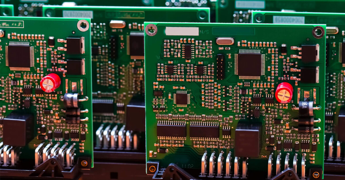
Use Quality Materials
Skimping on materials, usually costs in the long run. Use standard, quality materials in your layer stack.
Use Standard Geometrical Board Shapes
If at all possible, design your board in the standard square and rectangular shapes. Unusual shapes, increase manufacturing costs significantly. Try to avoid internal cutouts to your Printed Circuit Board unless absolutely needed.
Stay Within Minimum Spacing Requirements
As spacing between copper feature like pads and tracks decreases, the more manufacturing costs increase. The more packed into a smaller package, the more precise the manufacturing processes will be required. Many fab houses have a standard set of spacing requirements, which is somewhere around 8-10 mils minimum spacing between pads, tracks and track widths. Check with your manufacturer to see their specific spacing requirements. And save yourself from some added worry about adding design rules in your Printed Circuit Board (PCB) Design software for these spacing requirements so you don’t need to think about it while you design.
Use the Largest Diameter Possible for Holes
The smaller the holes and annular rings, the higher you’re the manufacturing costs. Again, it comes down to smaller spacing needing more precise machinery.
Use the Right Via for the Job
There are three types of vias
- through-hole
- blind
- buried
Blind and buried vias should only be used when absolutely needed – for high density and high frequency PCBs.
Avoid Extra Layers
Before adding additional layers for more routing space, power planes, or performance, think again. The difference between a four layer board and a two layer board is double. Only use as many layers as needed, even if it means making the board size a little larger.
Create your Design for Panelization
PCBs are manufactured on large production panels with other like PCBs. One can save money by using the largest panel size available from your manufacturer. In assembly maximizing the number of PCBs on a panel means that rapid-fire pick and place machine can operate much more efficiently, avoiding additional machine set-up time.
Use Industry Standard Sizes and Components
There’s a reason why the electronics industry uses a standardized set of sizes and components – it makes everyone’s job easier and more efficient. It also adds some potential for automation in all of those high-tech pieces of manufacturing equipment. So to extra costs, stick with industry standard parts.
Employ Surface Mount Components If Possible
Using surface mount components reduces the amount of holes that need to be drilled on a board. This also reduces the number of processes required to soldered components onto your board.
If you do decide to go with a mixed-component technology with both surface mount and through-hole parts, then prepare for some added costs. This type of setup will require multiple passes through the soldering oven and some manual hand assembly. If unavoidable, then try to keep all surface mount parts on one side of the board.
Ten tips to save you money when you need to get your next PCB fabricated and assembled.