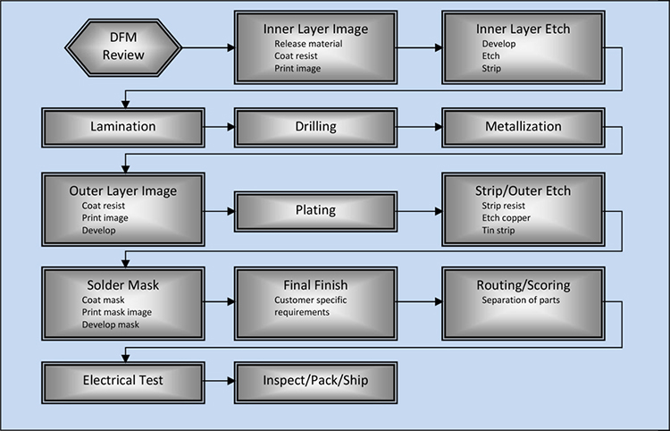
Prior to the start of Printed Circuit Board (PCB) manufacturing, engineers review all drawings, specifications and files to ensure manufacturability. Any identified concerns or issues or communicated back to the customer for clarification or correction. Once complete and all issues or concerns are resolved, the first step of the manufacturing process is to release material to etch the inner layer circuit patterns.
Patterning | Etching – Photoengraving
The inner layer copper coated laminated is coated with resist, photoengraved and developed. Afterward, the unwanted copper is etched off, and the remaining photo resist removed. This is considered a subtractive photoengraving process.
Lamination
PCBs are made up of multiple layers, consisting of several thin etched boards or trace layers which are bonded together through lamination (via heat and pressure). Once pressed or laminated together, the inner layer stack is drilled to add interconnections.
Drilling
Small holes or vias are precision drilled in the layers using numerically controlled drilling (NCD) machines and CAD files (excellon files). These files define the size and position of each via in the design.
Controlled depth holes or vias can be used to drill just one layer of the circuit board rather than drilling through all the layers. This is accomplished by drilling individual sheets or layers of the PCB prior to lamination. Vias which connect a layer to the outside surface of the Printed Circuit Board are called “blind vias.” Vias that only connect interior layers (not to an outside surface) are called “buried vias.” Via or hole walls are copper plated to connect conductive layers of printed circuit boards.
Metallization – Solder Plating | Solder Resist
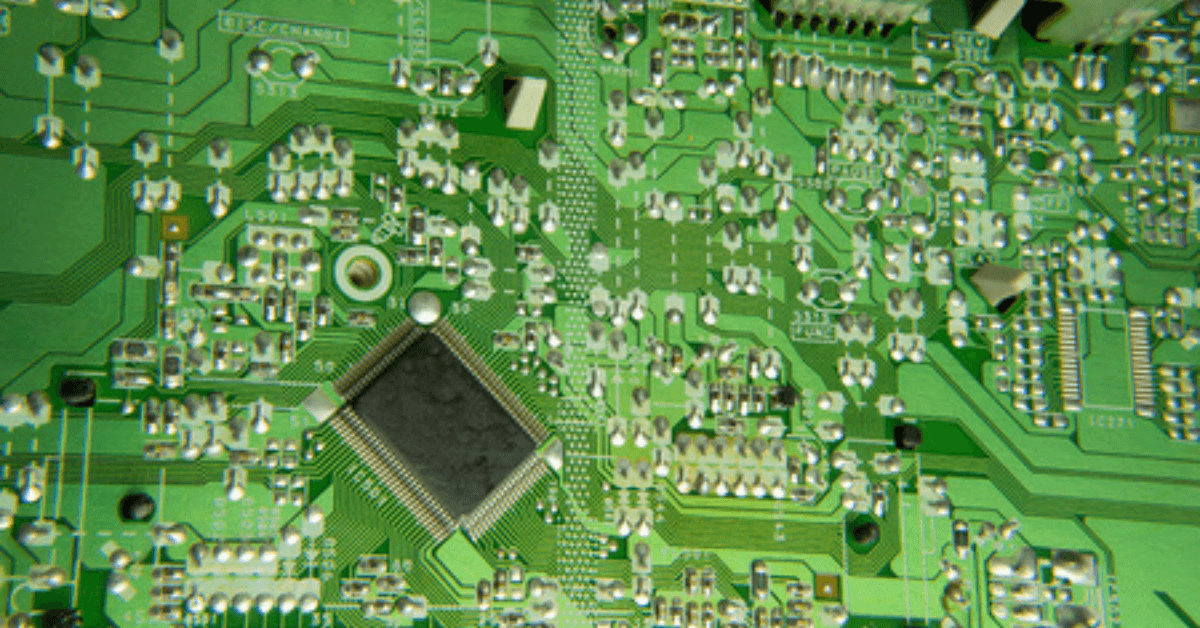
To enable electronic components to be mounted or soldered, metal “pads” and “lands” are required. Bare copper is not readily solderable, so it requires plating with a solderable material. Historically, lead based tin has been used for plating laminate surfaces. However, now due to environmental regulations newer materials are being used such as nickel, gold, or tin to offer solderability and compliance with new standards.
Areas that should not be soldered are covered with a material to resist soldering. Solder resist refers the a polymer coating that acts as a mask, thereby preventing solder from bridging traces and possibly creating short circuits to nearby component leads.
Outer Layer Fabrication
The above pattern etching (photoengraving, drilling and metallization steps) are also performed on the outer layer circuits. Following metallization of the outer layers final finishing is performed. Generally this includes application of solder mask, silk screen, testing and packaging.
Final Finishing
Solder Mask
The processed laminates are coated with solder mask and cured or developed usually via UV curing.
Silk Screen
Silk screen may be added to apply information to the outside surfaces of a printed circuit board. This usually includes component designator information and other relevant information such as logos, part numbers or manufacturer’s identification or specification information.
Testing
Unpopulated circuit boards are subjected to a bare board test where each circuit connection is verified by sending a small current through each contact point. Testers typically are “bed-of-nails” or “flying-probe type to make contact with the copper lands or holes on one or both sides of the board.
Routing
NC routing machines or scoring machines are used to aid is separation of the circuits from a manufacturing panel as specified by individual customer requirements prior to final packaging and shipment.