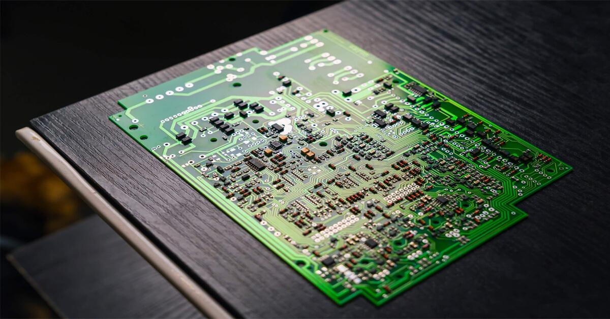
It’s the goal of all SMT assembler to minimize all solder joint defects. Only through understanding of defect root causes, and their prevention can improvements in product quality be realized and sustained. The top three (3) assembly defects, accounting for up to three quarters of all defects (according to industry statistics) are solder opens, shorts (bridging) and placement misalignment (due to shifting).
Open Solder Joints (34%), occur when there is a lack of an integral bond between the component lead and PCB pad, or other point of connection on a PCB. These types of defects can occur when solder appears only on the PCB pad while not on the component lead (or vice versa).
| Root Causes | Prevention |
|---|---|
| Lack of solder paste, or inconsistent deposit of paste | Ensure correct aspect ratio (aperture width to stencil thickness ratio) |
| Separation or gap between the PCB pad and component lead | PCB design and placement |
| Contamination or corrosion at component lead or PCB pad | Lead co-planarity and operator material handling procedures |
| Solder paste activity | Solder past contamination due to extreme environmental exposures |
| Reflow profile, no allowing all surfaces to reach reflow temperature | PCB fabrication issues |
Shorts (15%), also called Solder Bridging, occurs when solder is improperly crossing and connects one lead to another. This can be microscopic in size and difficult to detect. If undetected, it can cause serious damage to the circuit assembly, like a burn-up or blow-up of a component and/or burn-out PCB trace.
| Root Causes | Prevention |
|---|---|
| Reflow profile error (initial ramp rate too steep) | Ensure correct reflow profile |
| Solder pads too large relative to isolation between pads | Use appropriate solder past metal to flux weight ratio for the application. |
| Excess solder on pads due to incorrect stencil specification | Ensure paste deposition is in proper resolution and quality (no slump or smear) before reflow. |
| Inactive solder paste | Reduce stencil aperture dimensions by 10% or thickness of stencil to reduce amount of paste deposited |
| Poor seal between stencil and board during printing Misalignment between stencil and PCB | Verify alignment of stencil apertures to pads |
| Improper component placement of poor relationship between component lead to PCB pad size | Ensure proper pressure and accuracy for component placement. |
Component shift (15%), or misalignment of an item to its target. Component shifts occur during reflow due to the components ability to float on the molten solder. Components with many pads such as BGA components may realign themselves due to the surface tension of the molten solder, however many times the components will remain where they are placed, which is a good reason to make sure that components are placed exactly where they are supposed to be in the middle of the pad or land areas.
| Root Causes | Prevention |
|---|---|
| Mismatch in part to pad geometry causing the part to pull towards the closest thermal mass | Follow recommended PCB design guidelines |
| Mis-shaped or bent leads | Follow recommended temperature and humidity requirements from component manufacturers |
| Asymmetrical component heat sink | Improve accuracy of component placement machines and processes. |
| Excessive vibration or rapid speed changes in handling system | Minimize amount of movement due to conveyor or other handling processes |
| Poor solder deposition (wrong location, off pad, or incorrect volume) | Improve solderability of components or PCBs with appropriate flux |
| Incorrect convection rates (too high) | |
| Heating ramp rate too high causing outgassing of flux | |
| Small components placed next to large ones where heated gas is directed from the side of the large component towards a smaller one. |
PCBA failure is dependent on whether or not the assembly is considered a class 2 or class 3 products. IPC standards state that Class 2 products are expected to maintain continued performance and extended life as required, however uninterrupted service is desired but not critical. Class 3 products however, demand continued high performance or performance-on-demand is critical, and equipment downtime is unacceptable. Additionally, class 3 products may need to function in extreme environments, and the equipment must function when required, such as in life support or other critical systems. In either case, ensuring every assembly is of the highest quality and in proper working condition before leaving our shop will help to prevent latent failures.
To discuss how Optima can assist you with your design and design for manufacturing review to minimize the opportunity for PCB assembly defects, please let us know a good time to schedule a call, or send your email to optima@optimatech.net.